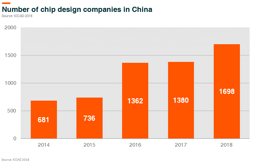
China’s Chip Design Ambitions
In the Right Place at the Right Time
Chip1 design (fabless) business is relatively easy to localize, thanks to
- the mature ecosystem support around the fabless, which has evolved over the years;
- strong domestic integrated circuit demand and domestic firms with advantages in client relationship building; and
- rich and young talent pool.
In this article, we explore the path of rising Chinese chip design companies.
Rise of domestic fabless gives Chinese chip companies cost advantage
The development of the fabless model separates design and the production of chips, which greatly reduces the capital expenditure burden on chip design companies, and provides them with flexibility in capacity expansion. The rapid growth of domestic foundries likes SMIC and Hua Hong, the two largest mainland Chinese foundries by revenue, and we also bring abundant capacity to serve the growing demand of the domestic chip design industry.

Rise of ARM (ARM holdings) and other chip architecture lowers the entry barrier to chip design
ARM licenses its architecture and core design for fabless companies to innovate on top of their foundation. This lowers the barriers to enter the chip design business, which allows Chinese chip design companies to ramp up quickly. Alternative open-source instruction sets like RISC-V are open-sourced, which also allows domestic chip design companies to innovate with low sunk costs.
Strong domestic demand, customer relationship —Advantages for local firms compared to foreign players
In 2019, China imported US$305.6Bn worth of integrated circuit (I.C.) products. China is the largest single-country market in semiconductor end demand, representing 34% of global semiconductor consumption in 2018, according to SIA. Today many terminal companies in consumer electronics, home appliances, and even new E.V. companies are based in China. Domestic fabless are able to build better customer relationships and work closely with companies to develop new chips. Local firms are also more willing to support Chinese chip design companies.
Domestic talent pool compared to foreign firms
New Chinese chip design companies are able to draw talents from three key talent pools:
- experienced overseas Chinese/Chinese ethnic engineers from leading global companies;
- experienced engineers from leading domestic companies like Huawei;
- 200,000 local I.C. design graduates every year and Chinese overseas graduates.
Our research suggests many domestic chip design companies have a core group of experienced engineers (most from mature design houses) who lead a team of young local engineers. We believe this process will train up domestic graduate talents quickly. In 2018 there were around 200,000 undergraduate students in I.C. related subject, among whom 38,000 entered the industry. Tsinghua University, Peking University, and Fudan University are top universities in China in this field. As compensation package and career development opportunities increase in the domestic I.C. design industry, more graduates will choose to join the industry.
Rise of local chip design leaders
We explore the backgrounds of key local chip design companies below to shed some light on the rise of Chinese fabless.
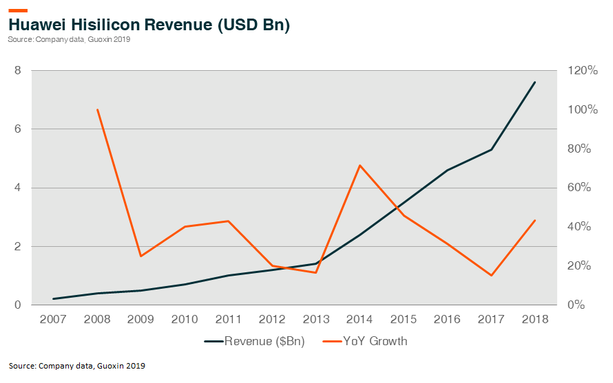
Huawei
Huawei established its first ASIC design center in 1991. The company launched its first ASIC chip in 1993. In 2004 Huawei established Hisilicon as a fabless subsidiary focusing on I.C. design. Huawei was able to leverage its strong vertical capability with presence in both telecom and consumer electronics equipment to incubate its in-house chip design company. Hisilicon now has over 7,000 employees with over 200 chipsets and 8,000 patents.
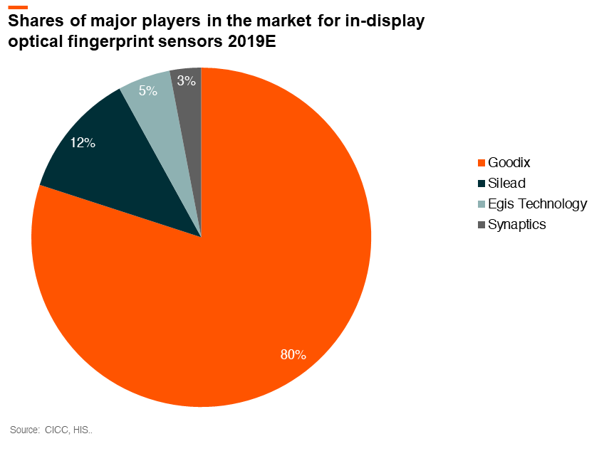
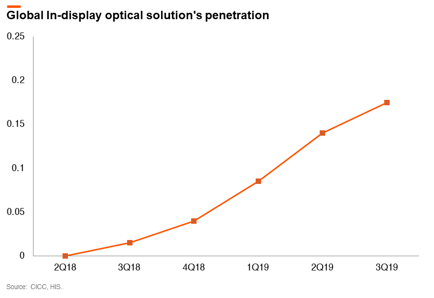
Goodix
Zhangfan, the founder of Goodix, is a locally trained engineer. He worked in the satellite navigation system R&D before joining the I.C. design industry. In 2002, Mr. Zhang founded Goodix, which initially focused on fixed-line telephone chips. Goodix is now a leader in the market for in-display optical fingerprint sensors. The company has a first-mover advantage in ultra-thin and in-display optical fingerprint sensors. In 2018, the company became the ‘world’s first chip designer to achieve commercial applications for in-display optical fingerprint sensors.
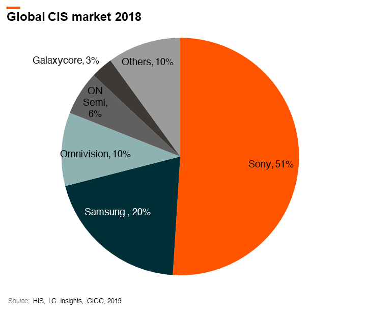
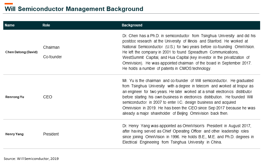
Will Semi
The company acquired OmniVision (O.V.) in August 2019. O.V. is the third-largest CIS design house with around 10% market share in the overall CIS market in FY18. The company adopts a fabless model and is currently working with four foundries includes TSMC, SMIC, Huali, Powership. Its backend suppliers include Xintec, VisEra, and KYEC. Around 70% of O.V.’s FY20 revenue is expected to come from smartphone CIS followed by 12% in surveillance and 10% in an auto.
Despite OmniVision being an U.S. company, the core founding team was mostly Chinese or Chinese ethnic background graduates from Tsinghua University. The founder of Will semi also graduated from Tsinghua University.
Capturing the Opportunities of Chinese Chip Industry
Improving and more open ecosystem development combined with better domestic support has paved the way for more domestic chip design companies to grow. Pioneer companies like Hisilicon showed the way for new Chinese chip design companies as well as training many Chinese chip design engineers. We continue to be positive about the future of China’s chip design industry and see many more companies rising in the future.
Global X China Semiconductor ETF (3191 HKD / 9191 USD) is designed to offer investors to access high growth potential through companies critical to the development of semiconductors in China.
Other Key Features:
- Targeted Exposure: The fund delivers targeted exposure to an emerging theme and industry.
- ETF Efficiency: In a single trade, the fund delivers access to dozens of companies with high exposure to the semiconductor theme in China.
Please click here for more information on the Global X China Semiconductor ETF.