Important Information
Investors should not base investment decisions on this material alone. Please refer to the Prospectus for details including the product features and the risk factors. Investment involves risks. Past performance is not indicative of future performance. There is no guarantee of the repayment of the principal. Investors should note:
- The investment objective of Global X China Semiconductor ETF’s (the “Fund”) is to provide investment results that, before fees and expenses, closely correspond to the performance of the FactSet China Semiconductor Index.
- The Fund is exposed to concentration risk by tracking a single region or country.
- The Index constituents may be concentrated in a specific industry or sector, which may potentially more volatile than a fund with a diversified portfolio.
- Semiconductor industry may be affected by particular economic or market events, such as domestic and international competition pressures, rapid obsolescence of products, the economic performance of the customers of semiconductor companies and capital equipment expenditures.
- Investment in Emerging Market, such as A-share market, may involve increased risks and special considerations not typically associated with investments in more developed markets, such as liquidity risk, currency risks, political risk, legal and taxation risks, and the likelihood of a high degree of volatility.
- The Stock Connect is subject to quota limitations. Where a suspension in the trading through the Stock Connect is effected, the Sub-Fund’s ability to invest in A-Shares or access Mainland China markets through the programme will be adversely affected.
- Listed companies on the ChiNext market and/or STAR Board are usually subject to higher fluctuation in stock prices and liquidity risks, over-valuation risk, differences in regulation, delisting risk, and concentration risk.
- There are risks and uncertainties associated with the current Mainland China tax laws, regulations and practice in respect of capital gains realized via Stock Connect on the Fund’s investments in Mainland China. Any increased tax liabilities on the Fund may adversely affect the Fund’s value.
- The trading price of the Fund’s unit on the SEHK is driven by secondary market trading factors, which may lead to a substantial premium or discount to the Fund’s net asset value.
- The Fund’s synthetic replication strategy may invest up to 50% of its net asset value in financial derivative instruments (“FDIs”), which may expose the Fund to counterparty/credit risk, liquidity risk, valuation risk, volatility risk and over-the-counter transaction risk. The Fund may suffer losses from its usage of FDIs.
- The Manager may at its discretion pay dividends out of the capital of the Fund. Distributions paid out of capital, represent a return of an investor’s original investment or its gains and may potentially reduce the Fund’s Net Asset Value per Share as well as the capital available for future investment.
- The Fund may suffer from a losses or delays when recovering the securities lent out. This may potentially affect its ability to meet payment and redemption obligations. Collateral shortfalls due to inaccurate pricing or change of value of securities lent, may cause significant losses to the Fund.
- The investment objective of Global X China Little Giant ETF (the “Fund”) is to provide investment results that, before fees and expenses, closely correspond to the performance of the Solactive China Little Giant Index.
- The Fund is exposed to concentration risk by tracking a single regions or countries.
- The Fund may invest in small and/or mid-sized companies, which may have lower liquidity and their prices are more volatile to adverse economic developments.
- Investment in Emerging Market, such as A-share market, may involve increased risks and special considerations not typically associated with investments in more developed markets, such as liquidity risk, currency risks, political risk, legal and taxation risks, and the likelihood of a high degree of volatility.
- The Stock Connect is subject to quota limitations. Where a suspension in the trading through the Stock Connect is effected, the Sub-Fund’s ability to invest in A-Shares or access Mainland China markets through the programme will be adversely affected.
- Listed companies on the ChiNext market and/or STAR Board are usually subject to higher fluctuation in stock prices and liquidity risks, over-valuation risk, differences in regulation, delisting risk, and concentration risk.
- There are risks and uncertainties associated with the current Mainland China tax laws, regulations and practice in respect of capital gains realized via Stock Connect on the Fund’s investments in Mainland China. Any increased tax liabilities on the Fund may adversely affect the Fund’s value.
- The trading price of the Fund’s unit on the SEHK is driven by secondary market trading factors, which may lead to a substantial premium or discount to the Fund’s net asset value.
- The Fund’s synthetic replication strategy may invest up to 50% of its net asset value in financial derivative instruments (“FDIs”), which may expose the Fund to counterparty/credit risk, liquidity risk, valuation risk, volatility risk and over-the-counter transaction risk. The Fund may suffer losses from its usage of FDIs.
- The Manager may at its discretion pay dividends out of the capital of the Fund. Distributions paid out of capital, represent a return of an investor’s original investment or its gains and may potentially reduce the Fund’s Net Asset Value per Share as well as the capital available for future investment.
- The Fund may suffer from a losses or delays when recovering the securities lent out. This may potentially affect its ability to meet payment and redemption obligations. Collateral shortfalls due to inaccurate pricing or change of value of securities lent, may cause significant losses to the Fund.
Why Huawei’s 3D chip design matters
In late May, Huawei announced a new semiconductor design roadmap dubbed “Logic Folding”. The core innovation is the introduction of 3D (three-dimensional) design into logic chip.
In traditional chip design, physical limitations dictated that transistors could only be fabricated on a single layer directly atop the wafer. The remaining layers were used merely to deploy copper interconnects, not transistors, which are the fundamental drivers of chip performance.
However, Huawei devised a method to bond two wafers using ‘hybrid bonding’ technology. This architecture aligns the two transistor-embedded wafers to face each other like a sandwich, with copper interconnect layers placed precisely at the central junction. In short, this enables the total number of transistors to double within the same physical footprint.
According to Huawei, this approach improves transistor density by 50% and power efficiency by 40% without using EUV equipment. Applying this technology enables the production of 3nm-class semiconductors using only a 7nm node. Furthermore, Huawei presented a roadmap to evolve its 3D design beyond two layers to three and four layers, aiming to produce 1.4nm-class semiconductor chips by 2031.
Its implication extends far beyond Huawei, carrying profound significance for the entire Chinese semiconductor industry. These implications can be summarized into three core questions.
- Huawei’s announcement actually credible?
- What impact on the entire Chinese semiconductor industry?
- what implications does this hold for global investments?
1. Is Huawei’s Announcement Actually Credible?
No cutting-edge technology can be entirely guaranteed of success at the mass-production stage.
However, looking at Huawei’s past track record, the fact that they have publicly announced this technology indicates that substantial preparations are already in place. For instance, when Huawei announced the mass production of its 7nm chip in August 2023, many experts raised doubts, arguing that while it was theoretically possible, it was practically unfeasible. Yet, Huawei succeeded in actual mass production.
Of course, skepticism and criticism regarding Huawei’s current design technology remain high. Solving thermal dissipation and yield issues during mass production will be far from easy.
Nevertheless, He Tingbo, Huawei’s semiconductor head, claim that it has verified 381 chips over the past six years for 3D design warrants close attention. Here, “381 chips” does not mean they tested 381 chips produced from the same design. It means they placed orders with a semiconductor fab for 381 entirely different design to produce. In semiconductor terminology, this is called a “Tape-out.”
Generally, a single tape-out for a new chip design costs several tens of millions of dollars. In the case of Nvidia in the United States, the company typically conducts only 1~2 tape-outs at Taiwan’s TSMC fab when announcing a new chip. In contrast, the fact that Huawei manufactured 381 different prototype chips means they injected several billion dollar over the past six years just to validate this 3D architecture. It is highly probable that through this process, Huawei acquired significant know-how to resolve thermal and yield issues to some degree.
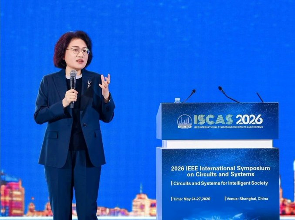
“Logic Folding” announcement by He Tingbo, the president of Huawei’s semiconductor biz
The wait to confirm its commercial viability will not be long. Huawei has already decided to apply this 3D design technology to its new Kirin smartphone chip slated for release this autumn. It is right around the corner. For external observers, the success or failure of Huawei’s new technology will be verifiable in the near future.
2. What Impact on the Chinese Semiconductor Industry?
In conclusion, the shift toward 3D chip design has a broader impact on the Chinese semiconductor supply chain. The Global X ETF suite includes several relevant ETFs positioned to benefit from this expanded market opportunity:
The significance of Huawei’s 3D technology extends far beyond an individual corporate achievement. From the perspective of the entire Chinese semiconductor industry, this 3D technology plan holds immense meaning.
Essentially, it buys the Chinese semiconductor industry roughly five years of time. If Huawei succeeds in mass-producing 3D logic chips, the Chinese semiconductor industry can narrow, or at least maintain, the technical gap with the US-centric supply chain until 2031.
Prior to this announcement, the Chinese semiconductor industry was stuck with 5nm as its most advanced process and 7nm as the node capable of mass production. On the other hand, TSMC plans to start mass production of its 1.4nm-class process by 2028. If this trend continues, the semiconductor gap between China and the US will widen severely by around 2030. In that scenario, no matter how loudly China advocates for semiconductor localization, its products are highly likely to be rejected by the market. If the gap between the two processes is 5nm versus 1.4nm, the actual chip performance gap widens by more than threefold.
However, if China advances to 3nm-class performance by 2028 and 1.5nm-class by 2031 through 3D semiconductor mass production, it can lock the performance gap with TSMC to a 1.5-fold level. Consequently, China secures a five-year buffer until 2031. In the meantime, the possibility remains open for China to self-develop EUV equipment, which is currently considered its greatest weakness.
Meanwhile, from a broader perspective, Huawei’s announcement aligns perfectly as an integral part of the broader Chinese semiconductor technology road map.
The grand objective is the three-dimensionalization of all semiconductor designs. This is not confined strictly to Huawei’s logic chip sector. The memory sector, whose importance is increasingly emphasized these days, also views 3D design as the sole alternative for technological advancement.
What is striking here is that China is not lagging behind the global leader in 3D process technology. The core technology for 3D semiconductor production is ‘hybrid bonding’, a technology that directly connects two wafers through the molecular bonding of copper interconnects and insulation layers without adhesives.
Indeed, it is an interesting fact that the first company in the world to introduce hybrid bonding into NAND sector was China’s YMTC (Yangtze Memory). Also, CXMT (Changxin Memory) is currently actively pushing forward with 3D DRAM development. According to a report by tech media outlet Tom’s Hardware, industry analysis suggests that YMTC’s hybrid bonding technology is flowing into CXMT to facilitate this transition. Huawei has also forged a tight technological alliance with YMTC and CXMT.
In other words, YMTC’s hybrid bonding know-how is being shared across the entire Chinese semiconductor industry. Huawei’s ability to announce ‘Logic Folding’ was likely made possible due to this accumulation of hybrid bonding technology within the Chinese ecosystem.
| Company Name | Critical Tech / Equipment | China Semiconductor (3191 HK) |
GX China Little Giant (2815 HK) |
Note |
|---|---|---|---|---|
| Piotech | Wafer-to-Wafer (W2W) Hybrid Bonders | Y | Y | Direct Play on 3D chip. Supplies the precise bonding tools required to fuse twin transistor layers at a molecular level. |
| Hwatsing | Chemical Mechanical Planarization (CMP) tools | Y | Y | The ultimate enabler of Hybrid Bonding. Fusing wafers without adhesives requires an atomic-scale flat surface. Holds a dominant position in domestic CMP tools. |
| ACM Research | Tahoe Single-Wafer Cleaning tools Ultra-high-frequency Megasonic systems |
Y | Y | Micro-particles create destructive voids during 3D binding. Advanced package cleaning tools protect target yield rates. |
| Anji Micro | Advanced Tungsten & Copper CMP Slurries Post-CMP Cleaning Chemicals |
Y | Y | The recurring OPEX play on 3D scaling. Supplies the highly guarded chemical formulations that enable atomic flat bonding. |
| NAURA | Atomic Layer Deposition (ALD) Advanced Plasma Etching Ultra-fine Copper Interconnects |
Y | – | Critical for etching between sandwiched wafers. The bellwether of Chinese semiconductor self-reliance. |
| AMEC | Capacitively Coupled Plasma (CCP) Etchers Inductively Coupled Plasma (ICP) Etchers |
Y | – | Specializes in deep, high-aspect-ratio etching needed to connect copper wires through the insulation layers. |
(Source) Bloomberg, Mirae asset Global Investments (HK), date of 29 May 2026
3. What Implications Does from an Investment Perspective?
Equipment firms essential for the 3D process, such as hybrid bonding, are already gaining traction in the market. A prime example is Piotech, which possesses a comprehensive lineup of wafer-to-wafer (W2W) and die-to-wafer (D2W) hybrid bonding equipment. In addition, NAURA and AMEC, which possess ultra-fine wafer surface control and etching technologies—both critical prerequisites prior to hybrid bonding—are also cited as major beneficiaries. Furthermore, Hwatsing, a small-cap leader in chemical mechanical planarization (CMP) that flattens wafer topography at an atomic level before 3D bonding, and ACM Research, a leader in cleaning equipment that perfectly removes contaminants right before bonding was often mentioned.
From a broader perspective, this announcement signifies a one-step expansion of the growth potential of the Chinese semiconductor industry. Historically, China’s semiconductor industry has demonstrated growth along two main pillars.
First, it has steadily expanded its global market share in legacy nodes, analog, and power semiconductors. Originally, this sector was far removed from the AI semiconductor trend, and aggressive capacity expansions by Chinese firms previously triggered oversupply concerns. However, the recent explosion of AI data centers has created an inverse effect, causing massive demand for power semiconductors and analog chips to spill over into legacy process areas. Because major semiconductor corporations in the US and South Korea are focusing their resources exclusively on cutting-edge AI chips, the global production capacity for legacy node chips has relatively decreased, creating a structural windfall for Chinese companies.
Consequently, global legacy foundry utilization rates, which hovered around 75% in 2025, have sharply rebounded to the 90% range. The utilization rate of SMIC, China’s largest foundry, is nearing 95%, while Hua Hong, which primarily produces power semiconductors and analog chips, has seen its utilization rate exceed 100%.
Second, China is benefiting heavily from the demand for AI inference semiconductors. As the AI market evolves from the training phase to the inference phase, the demand for AI inference semiconductors has surged significantly. In the AI training chip market, Chinese semiconductors struggle to compete with global leaders due to the technological gap. However, inference chips can be sufficiently manufactured even within China’s 7nm fabs. In fact, Huawei’s next-generation AI inference chip, the ‘Ascend 950PR’, and its subsequent models, which entered full-scale mass shipment stages this year, are currently recording high market shares, to the point where domestic supply cannot keep up with surging demand.
On top of this, Huawei’s latest announcement of ‘Logic Folding’ adds a new tier of growth potential for the nation. This implies that in the high-end semiconductor sector, which was previously bottlenecked at the 7nm (logic) and 1a-nanometer (DRAM) levels, the Chinese supply chain can now directly track the global leaders. As a result, its total addressable market (TAM) is widening.
In conclusion, the shift toward 3D chip design has a broader impact on the Chinese semiconductor supply chain. The Global X ETF suite includes several relevant ETFs positioned to benefit from this expanded market opportunity:
Global X China Semiconductor ETF (3191 HK) delivers 100% pure-play exposure to the domestic chip ecosystem, while Global X China Little Giant ETF (2815 HK) maintains a significant tech-localization allocation with a semiconductor weight exceeding 40%.